 Startups Bring Optics Right to the GPU New optical interconnects could provide the bandwidths needed for AI data centers
If you pack too many copper wires together, eventually you’ll run out of space—if they don’t melt together first. AI data centers are encountering similar limitations with the electronic interconnects that shuttle data among GPUs and memory. Accommodating the data-guzzling demands of AI means the industry is turning to bigger chips with more processors, which means denser connectivity across longer distances within a rack. Startups are unveiling demonstrations of how GPUs can shed their copper interconnects, replacing them with optical links.
Optical links are no stranger to data centers. They traffic data between racks, using pluggable transceivers that convert electrical signals into optical ones. To improve energy efficiency, “integrating optics into chip packages has been a holy grail,” says Clint Schow, an electrical engineering professor at the University of California, Santa Barbara. That’s co-packaged optics, or CPO, and tech behemoths are throwing their weight behind it. Nvidia recently announced production of a networking switch using photonic modulators embedded onto the same substrate as the switch. “That rocked the industry,” says Bardia Pezeshki, CEO of Sunnyvale, Calif.–based startup Avicena.
Nvidia’s announcement is exciting because it brings photonics inside the rack, explains Keren Bergman, an electrical engineering professor at Columbia University and cofounder of Xscape Photonics. But Nvidia plans to bring photonics only to the network switch (for now!). Avicena and other startups are challenging the notion that optics doesn’t have the cost, reliability, and power efficiency to replace copper within a rack. They’rebringing optical interconnects directly onto GPU and memory packages. Even these final meter-long links need more bandwidth than copper can provide, Bergman says. The same basic technology “can go right next to the GPU,” bringing the optics closer to the data source and allowing them to carry bandwidth off the chip package itself.
Pradeep Sindhu, cofounder of Juniper Networks and Fungible, now at Microsoft, offers a skeptical view. In clusters where you want flexible point-to-point links between large numbers of GPUs, the granularity of each switchable data lane matters. One fat pipe between point pairs won’t suffice. Rather, you want many smaller pipes, and too much bandwidth per fiber reduces flexibility. For example, the lofty goal of connecting 512 GPUs, each linked by 200-gigabit-per-second lanes to 64 switches requires more than 30,000 connections. “If you jam 16 wavelengths down a single fiber how do you connect this many GPUs to this many switches?” Sindhu says. Fewer, more powerful switches that electronically parse the fat pipes is one answer—but that swaps redundancy for single-point failure. Moreover, multiwavelength lasers pose concerns about cost, energy efficiency, and reliability.
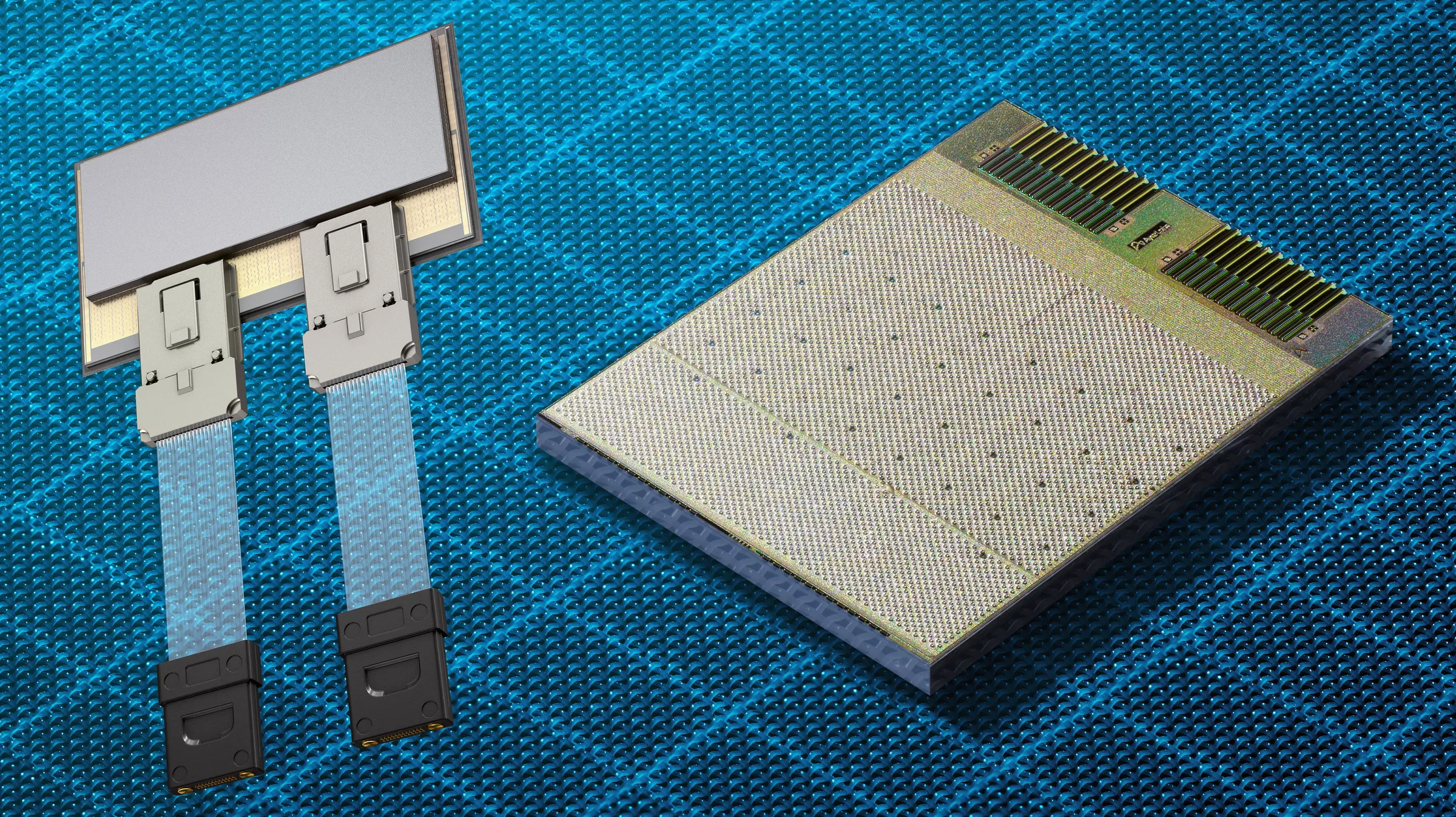
Another approach skirts both problems. Avicena uses hundreds of blue microLEDs connected through imaging fibers to move data. Pezeshki explains, “If you have a camera look at a TV, you have an optical connection with no lasers involved.” Avicena’s optical chiplet has a small microLED display and a tiny camera, with a mind-boggling frame rate, announced in the modular LightBundle platform based on a frame rate of 10 gigabits per second per lane. Each display of 300 microLEDs carries an accumulated 3 Tb/s, but with high granularity. Eliminating lasers reduces the reliability risk, cost, and complexity, and gains a fivefold energy improvement according to Pezeshki. Sindhu says, “I am optimistic that microLEDs are the leading technology.”


